
Manufacturing Complexity Comparison Tool
Process Depth
Number of distinct steps required from raw material to finished product.
Precision Level
Tolerance and feature size (nanometers vs. millimeters).
Environmental Control
Cleanroom class, temperature, vibration, and humidity stability.
Capital Intensity
Investment in equipment, facilities, and R&D.
Supply Chain Interdependence
How many specialized vendors and materials are needed.
Comparison Table: Complexity Metrics Across Industries
| Process | Typical Feature Size | Number of Steps | Cleanroom Class | Capital Investment (USD) | Complexity Rating |
|---|---|---|---|---|---|
| Semiconductor fabrication (7 nm node) | 7 nm | >200 | Class 1 | $12 billion (fab) | Highest |
| Aerospace frame & engine | mm-scale (large-scale) | ~150 | Class 100,000 | $5 billion (assembly line) | High |
| Pharma biologics (MAb) | micron-scale bioreactors | ~120 | Class 10 | $2 billion (facility) | Medium |
| Nuclear reactor components | mm-scale steel | ~180 | Class 10,000 | $8 billion (plant) | Medium |
| Metal 3D printing (large parts) | 10-100 µm | ~100 | Class 100,000 | $500 million (printer fleet) | Low |
Why Semiconductor Fabrication Tops the List
- Wafer Preparation: Silicon crystals grown in Czochralski furnace, sliced to 200-300 mm wafers, polished to optical flatness.
- Photolithography: EUV light (13.5 nm wavelength) shines through masks onto photoresist layers with sub-nanometer accuracy.
- Etching & Deposition: Reactive-ion etching removes silicon; atomic-layer deposition (ALD) adds layers atom by atom.
- Cleanroom Environment: Class 1 cleanrooms require fewer than one particle per cubic foot larger than 0.5 µm.
- Automation & Robotics: Hundreds of robotic arms shuttle wafers with micron-level positioning.
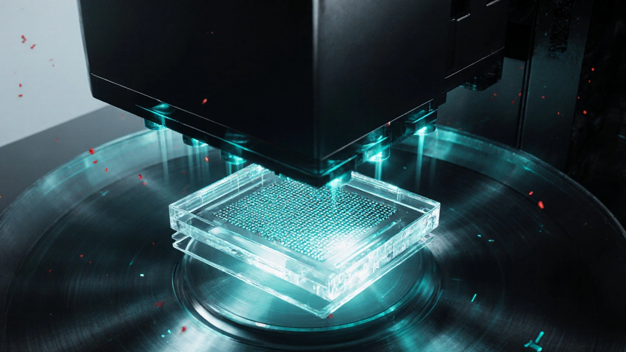
When people talk about the most complex manufacturing process, Semiconductor manufacturing is a high‑tech, multi‑step operation that builds tiny electronic circuits on silicon wafers. From ultra‑clean rooms to atomic‑scale lithography, every step demands precision, massive capital, and tightly coordinated supply chains. In this article we break down why chip fabrication tops the complexity chart, compare it with other heavyweight processes, and explain the challenges that keep it at the cutting edge of modern industry.
How to Judge Manufacturing Complexity
- Process depth: Number of distinct steps required from raw material to finished product.
- Precision level: Tolerance and feature size (nanometers vs. millimeters).
- Environmental control: Cleanroom class, temperature, vibration, and humidity stability.
- Capital intensity: Investment in equipment, facilities, and R&D.
- Supply‑chain interdependence: How many specialized vendors and materials are needed.
Top Contenders for the ‘Most Complex’ Title
Before we crown a winner, let’s look at the processes that regularly appear in the debate.
- Semiconductor fabrication - sub‑10nm photolithography, dozens of cleanroom steps, and billions of transistors per chip.
- Aerospace manufacturing - building aircraft bodies, engines, and space‑grade structures with strict weight and safety limits.
- Pharmaceutical biologics production - living cell cultures, sterile bioreactors, and rigorous validation for each batch.
- Nuclear reactor component fabrication - ultra‑pure metals, welding under inert atmosphere, and nuclear‑grade certification.
- Large‑scale additive manufacturing (metal 3D printing) - layer‑by‑layer sintering, real‑time monitoring, post‑process heat treatments.
Why Semiconductor Fabrication Beats the Rest
Let’s walk through the hallmark steps that illustrate sheer complexity.
- Wafer preparation: Silicon crystals are grown in a Czochralski furnace, sliced to 200‑mm or 300‑mm wafers, then polished to optical flatness. Any crystal defect can ruin thousands of chips.
- Photolithography - the true star of the show. A photolithography machine shines extreme ultraviolet (EUV) light (EUV lithography at 13.5nm wavelength) through a mask onto a photoresist layer. The pattern must be transferred with sub‑nanometer accuracy, requiring vibration‑free tables, temperature control within ±0.01°C, and complex light‑source chemistry.
- Etching and deposition: Reactive‑ion etching removes silicon where the resist was cleared, while atomic‑layer deposition (ALD) adds insulating and conductive layers atom by atom. Each cycle is timed to a few seconds.
- Mask making: The mask itself is a multi‑layer stack of opaque material and quartz, fabricated by electron‑beam lithography - a process that can cost over $1million per mask set.
- Inspection and metrology: After every major step, advanced scanners measure line widths, overlay accuracy, and defect density. Modern tools can detect a particle smaller than a virus.
- Cleanroom environment: The entire fab operates at Class1 or better (cleanroom - fewer than one particle per cubic foot larger than 0.5µm). Maintaining that purity requires HEPA/ULPA filtration, positive pressure, and strict gowning procedures.
- Automation & robotics: Hundreds of robotic arms shuttle wafers between tools with micron‑level positioning. Any mis‑alignment can cause a yield drop from 90% to 30%.
- Yield management: Even after successful processing, statistical process control (SPC) analyses millions of test results to pinpoint drifting parameters.
The cumulative effect is a process where a single defect can cost millions, and a single change demands months of re‑validation. That depth of inter‑dependency is unmatched.
Comparison Table: Complexity Metrics Across Industries
| Process | Typical Feature Size | Number of Steps | Cleanroom Class | Capital Investment (USD) |
|---|---|---|---|---|
| Semiconductor fabrication (7nm node) | 7nm | >200 | Class1 | $12billion (fab) |
| Aerospace frame & engine | mm‑scale (large‑scale) | ~150 | Class100,000 | $5billion (assembly line) |
| Pharma biologics (MAb) | micron‑scale bioreactors | ~120 | Class10 | $2billion (facility) |
| Nuclear reactor components | mm‑scale steel | ~180 | Class10,000 | $8billion (plant) |
| Metal 3D printing (large parts) | 10‑100µm | ~100 | Class100,000 | $500million (printer fleet) |
Key Challenges Engineers Face in Chip Fab
- Yield loss from tiny defects: A particle the size of a dust mote can short a transistor, so fab operators run continuous particle‑count monitoring.
- Tool uptime: Lithography machines have a mean‑time‑between‑failure of ~500hours; any downtime ripples through the schedule.
- Supply‑chain risk: Photoresist chemicals, ultrapure gases, and specialty silicon wafers are sourced from a handful of suppliers; geopolitical shifts can halt production.
- Energy consumption: A 300‑mm fab can draw >100MW, comparable to a small city, making sustainability a major focus.
- Skill shortage: Operators need expertise in optics, chemistry, robotics, and data analytics - a rare combination.
What the Future Holds
Even as we push toward 3‑nm and 2‑nm nodes, the complexity curve keeps rising. Emerging technologies like nano‑imprint lithography, AI‑driven process control, and quantum‑dot manufacturing promise new layers of intricacy. Companies that master the orchestration of thousands of interlocking steps will keep the title of "most complex" firmly in their hands.
Frequently Asked Questions
Why is semiconductor manufacturing considered the most complex?
It combines the highest number of steps, the tightest tolerances (sub‑nanometer), ultra‑clean environments, massive capital costs, and a supply chain that spans dozens of specialized vendors. A single defect can ruin millions of dollars worth of chips, so every micron‑scale operation is tightly controlled.
How does cleanroom class affect process complexity?
Lower cleanroom classes (e.g., Class1) allow fewer particles per cubic foot, which is crucial when patterns are measured in nanometers. Maintaining such an environment requires sophisticated filtration, strict gowning protocols, and constant monitoring, adding layers of operational difficulty.
Can aerospace manufacturing rival chip fab in complexity?
Aerospace involves large‑scale structures, stringent safety standards, and complex supply chains, but its feature sizes are orders of magnitude larger than semiconductor features. The number of steps and precision requirements are high, yet the nanometer‑scale control of chip fabs still surpasses aerospace in raw technical intricacy.
What role does AI play in modern fabs?
AI analyzes terabytes of sensor data in real time, predicts tool failures, optimizes recipe parameters, and improves yield. By turning vast data streams into actionable insights, AI reduces human error and helps manage the fab’s inherent complexity.
Is there a cheaper alternative to semiconductor fabs for high‑performance computing?
Emerging options like silicon photonics or advanced packaging can offload some functions from the die, but they still rely on traditional semiconductor processes for core logic. Until those alternatives mature, the classic fab remains the most complex-and indispensable-manufacturing route.