Photolithography: The Core Process Behind Modern Electronics
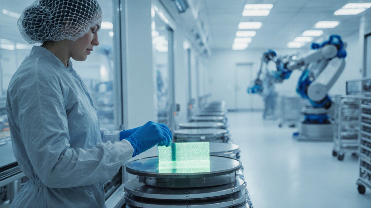
When working with Photolithography, a patterning technique that uses light to transfer geometric designs onto a substrate. Also known as optical lithography, it is the backbone of every silicon chip you touch. The process starts with a thin film of Photoresist, light‑sensitive material that hardens where light hits and washes away elsewhere. After coating, a mask bearing the circuit layout is aligned, UV light flashes, and the exposed resist forms the blueprint for etching. Key attributes include wavelength (193 nm lasers dominate), resolution (down to ~20 nm), and steps like coating, exposure, development, and strip. These steps together enable the trillion‑dollar semiconductor industry to shrink devices year after year.
Why Photolithography Matters Across Industries
The photolithography step is inseparable from Semiconductor Manufacturing, the full‑scale production of integrated circuits and MEMS devices. Without a clean, particle‑free Cleanroom Environment, a controlled space with filtered air and strict temperature limits, even the best mask can’t produce reliable patterns. The mask itself, crafted through precise Mask Making, the creation of photomasks that carry the circuit geometry for each wafer layer, is a critical cost driver and a source of competitive advantage. Together, these entities form a chain: photolithography requires a mask, the mask needs a cleanroom, and the cleanroom enables semiconductor manufacturing. Each link influences the others—advances in mask materials shrink feature sizes, which in turn demand tighter cleanroom specs and more sophisticated lithography tools.
Understanding this chain helps you make sense of the diverse articles below. Whether you’re reading about the biggest expense in manufacturing, the rise of India’s electronics sector, or the challenges of plastic waste, the same principles of precision, cost control, and material handling apply. Photolithography shows how a single high‑tech process can dictate equipment choices, labor skills, and even environmental impact across the supply chain. The posts that follow dig into those topics—from cost‑cutting strategies in factories to the global race for advanced electronics—offering practical insights that tie back to the fundamentals explained here. Dive in and see how the details of a light‑based patterning step echo throughout the whole world of modern production.
What Is the Most Complex Manufacturing Process?
Explore why semiconductor fabrication tops the list of complex manufacturing processes, comparing it with aerospace, pharma, and nuclear production, and learn the key challenges and future trends.
