Semiconductor Fabrication: What You Need to Know
If you’re curious about how the tiny chips inside your phone or laptop come to life, you’re in the right place. Semiconductor fabrication is the series of steps that turn raw silicon into the powerful processors that run modern tech. In this guide we break down the process, point out the biggest hurdles, and share tips you can use whether you’re a student, a startup founder, or just a tech‑enthusiast.
Key Steps in Chip Production
The journey starts with a pure silicon wafer. First, the wafer gets a thin layer of photoresist, which is a light‑sensitive material. A patterned mask then exposes the photoresist to ultraviolet light, creating the design of the circuit. After development, the exposed parts are etched away, leaving trenches that define transistors and interconnects.
Next comes doping, where the wafer is bombarded with gases to change its electrical properties. This step creates n‑type and p‑type regions that form the heart of each transistor. Once the doping is done, layers of metal are deposited to connect all the components. The wafer goes through multiple cycles of lithography, etching, doping, and metal deposition – often more than a dozen times – until the full 3‑D structure is built.
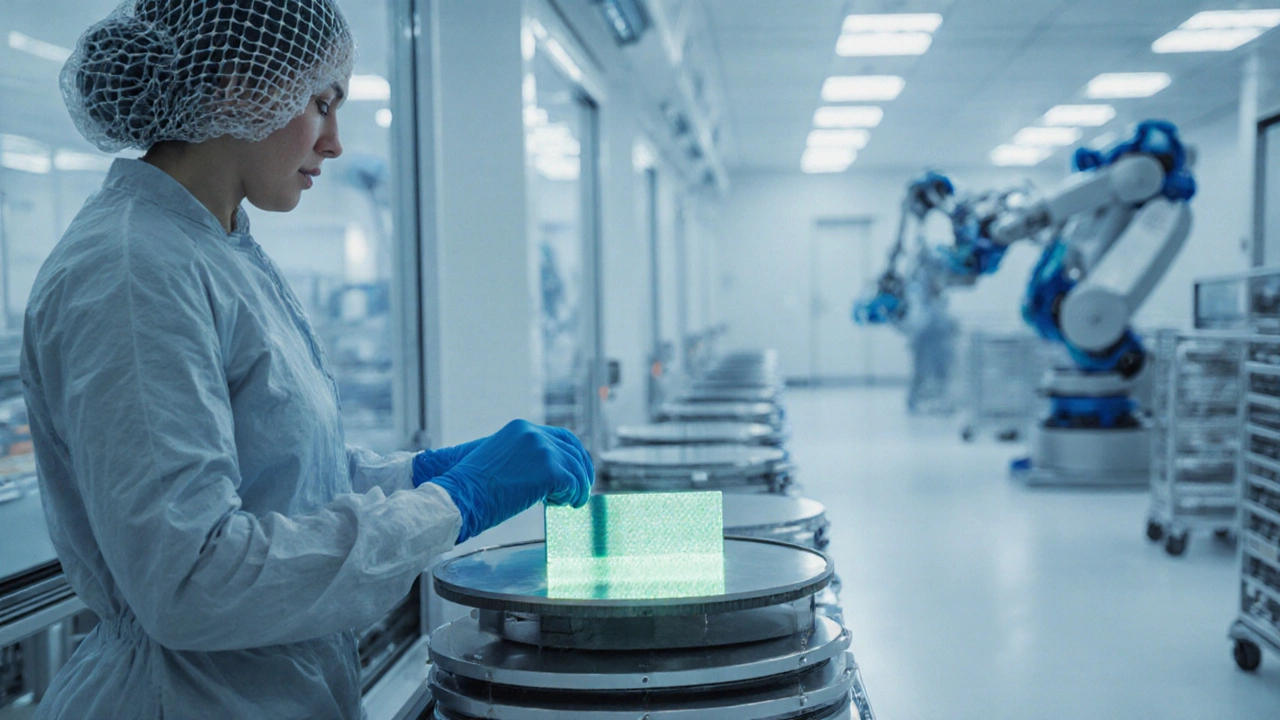
Finally, the wafer is tested, cut into individual chips (called dice), and packaged. Packaging protects the delicate silicon and adds the pins or bumps needed to plug the chip into a board. Each stage requires ultra‑clean environments called cleanrooms, where even a speck of dust can ruin a chip.
Current Challenges and Opportunities
One of the biggest headaches today is the shortage of high‑purity chemicals needed for etching and cleaning. Recent reports from India’s chemical sector show supply gaps that can slow down fab lines. Companies are looking to secure local sources or recycle chemicals to keep production moving.
Another challenge is the rising cost of equipment. Advanced lithography machines cost billions, and not every fab can afford the latest tools. This gap pushes some manufacturers to specialize in older nodes where the equipment is cheaper but still in demand for automotive and IoT devices.
On the upside, the push for greener manufacturing is opening new markets. Reducing water use, cutting energy consumption, and using sustainable materials are becoming must‑haves. Firms that adopt these practices can attract eco‑focused customers and even qualify for government incentives.
For startups, the takeaway is clear: focus on niche applications where you don’t need the most advanced node, partner with foundries that have spare capacity, and stay agile with supply chain options. Keep an eye on policy changes, especially in regions like India where the chemical industry is shifting fast.
Whether you’re planning a new product, studying for exams, or just love tech, understanding these basics gives you a solid footing in the semiconductor world. Stay curious, watch the industry news, and you’ll see how today’s challenges turn into tomorrow’s breakthroughs.
What Is the Most Complex Manufacturing Process?
Explore why semiconductor fabrication tops the list of complex manufacturing processes, comparing it with aerospace, pharma, and nuclear production, and learn the key challenges and future trends.
Most Difficult Manufacturing Processes: Inside Semiconductor Fabrication and More
A deep dive into the toughest manufacturing process in the world, exploring why semiconductor fabs are so complicated and what makes precision manufacturing so tough.
